Top 3 Powerful PCB Inspection Technologies: AOI, SPI and AXI Inspection Systems Explained
Introduction to PCB Inspection Technologies
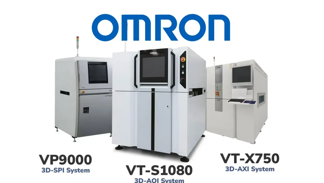
Printed circuit board (PCB) manufacturing has grown more complex as electronic devices shrink and demand for reliability increases. Ensuring every board performs flawlessly is now a mission-critical task for electronics companies. That’s where AOI, SPI and AXI inspection systems come into play.
These systems are the backbone of modern quality assurance in SMT production lines. Each serves a unique function—optical inspection, paste inspection, or X-ray detection—and together, they form a robust defense against defects.
What is AOI (Automated Optical Inspection)?
How AOI Works
AOI uses high-resolution cameras and lighting systems to visually inspect PCBs for defects. It captures 2D or 3D images of the board and uses software algorithms to compare them against a reference image.
Advantages of AOI Systems
- Speed & Efficiency: AOI systems can inspect hundreds of components in seconds.
- Non-contact inspection: There’s no risk of damaging delicate parts.
- Easy integration: AOI can be implemented post-SMT, post-reflow, or even at multiple stages.
Common Applications of AOI
- Detecting missing or misaligned components
- Solder joint inspection
- Polarity and orientation checks
Understanding SPI (Solder Paste Inspection)
The Importance of Solder Paste Inspection
Solder paste volume and placement are crucial for proper component bonding. A bad solder joint can mean product failure.
SPI Technology and Process
SPI systems use 3D laser scanning or structured light to measure the height, volume, and alignment of solder paste on PCBs. It works immediately after stencil printing but before pick-and-place.
Benefits of Using SPI
- Prevents soldering issues before they occur
- Quantitative feedback for printer calibration
- Supports process optimization and traceability
All About AXI (Automated X-ray Inspection)
What Makes AXI Different from AOI and SPI
AXI doesn’t rely on visible light. Instead, it uses X-ray technology to inspect hidden solder joints, such as those in BGA (Ball Grid Array) or QFN (Quad Flat No-lead) packages.
Key Features of AXI Systems
- 3D Tomography: Visualizes internal structures layer-by-layer.
- Void and crack detection: Ideal for critical applications.
- Non-destructive testing: Maintains board integrity.
Ideal Use Cases for AXI
- High-reliability sectors like aerospace and medical devices
- Complex multilayer boards
- BGA inspection where optical access is impossible
Comparative Analysis: AOI vs SPI vs AXI
When to Use Each Inspection Method
| Inspection Type | Ideal Stage | Best For |
|---|---|---|
| AOI | Post-Placement / Post-Reflow | Component presence, orientation |
| SPI | Post-Printing | Solder paste volume and alignment |
| AXI | Post-Reflow | Hidden solder joints and internal voids |
Cost, Speed, and Accuracy Comparison
- AOI is fastest and most economical.
- SPI is essential for early defect prevention.
- AXI is more expensive but unmatched in depth analysis.
Emerging Trends in PCB Inspection Systems
AI Integration and Machine Learning
Modern systems now include AI-driven defect classification to reduce false calls and improve accuracy. They also adapt over time to changes in production conditions.
Industry 4.0 and Smart Factories
AOI, SPI, and AXI systems are increasingly connected to MES (Manufacturing Execution Systems), enabling real-time feedback loops, predictive maintenance, and end-to-end traceability.
FAQs About AOI, SPI and AXI Inspection Systems
Q1: Why is it important to use multiple inspection systems in PCB manufacturing?
A1: Each system detects different types of defects—AOI checks visual flaws, SPI ensures paste quality, and AXI uncovers hidden problems. Together, they cover all possible issues.
Q2: Can AOI detect solder paste problems?
A2: Not effectively. AOI may see gross misprints, but SPI provides accurate volumetric data for solder paste.
Q3: Is AXI safe for operators and PCBs?
A3: Yes, AXI uses low-dose X-rays that are safe and non-destructive.
Q4: How does SPI improve production yield?
A4: By catching solder paste issues early, SPI reduces rework, improves first-pass yield, and saves money.
Q5: Are these systems expensive to maintain?
A5: AOI and SPI systems have moderate maintenance costs, while AXI systems may require specialized service due to their complexity.
Q6: Which industries rely most on AXI inspection?
A6: Aerospace, medical, automotive, and defense sectors where high-reliability PCBs are mandatory.
Conclusion: Choosing the Right PCB Inspection System
When it comes to AOI, SPI and AXI inspection systems, there’s no one-size-fits-all solution. The most effective manufacturing lines use all three in harmony to achieve maximum yield, reliability, and efficiency.
Whether you’re a startup building IoT devices or a major player in automotive electronics, investing in comprehensive inspection technology is no longer optional—it’s essential for staying competitive.


